
MAX 10 FPGA Development Kit
- Brand: Terasic
- Product Code: MAX 10 FPGA Development Kit
- Availability: In Stock
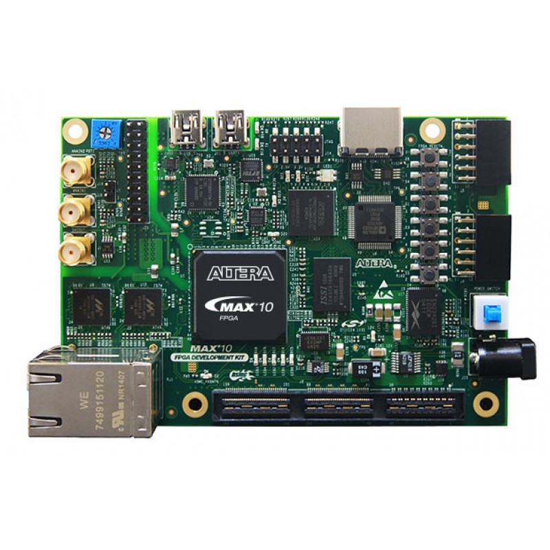
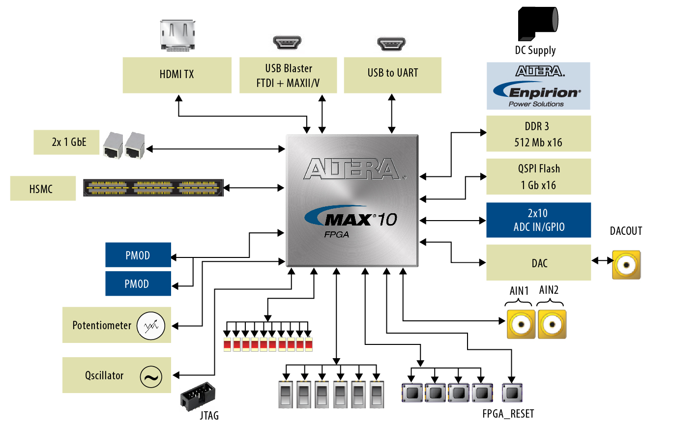
The Altera® MAX® 10 FPGA Development Kit provides a full featured design platform built around a 50 K logic elements (LEs) MAX 10 FPGA, optimized for system level integration with on-die analog-to-digital converter (ADC), dual-configuration flash, and DDR3 memory interface support. The board features on-board USB-BlasterTM II, high-speed mezannine card (HSMC), and Pmod™ Compatible expansion cards, high-definition multimedia interface (HDMI) output, and dual Ethernet for industrial Ethernet applications. The MAX 10 FPGA Development Kit provides the perfect system-level prototyping solution for industrial, automotive, consumer, and many other market applications.
With this development board, you can:
- Develop designs for the 10M50D, F484 package FPGA
- Measure the performance of the MAX 10 FPGA analog-to-digital block conversion
- Interface MAX 10 FPGAs to DDR3 memory at 300 MHz performance
- Run embedded Linux using the Nios® II processor
- Interface to daughtercards and peripherals using HSMC and Digilent Pmod™ Compatible connectors
- Measure FPGA power (VCC_CORE and VCC_IO ) using the power monitor graphical user interface (GUI)
- Reuse the kit’s PCB board and schematic as a model for your design
MAX 10 FPGA Development Board Block Diagram
Specifications
The MAX 10 FPGA Development Kit includes the following:
- RoHS- and CE-compliant MAX 10 FPGA development board
- Featured devices
- MAX 10 FPGA (10M50D, dual supply, F484 package)
- Enpirion® EN2342QI 4A PowerSoC voltage-mode synchronous step-down converter with integrated inductor
- Enpirion EN6337QA 3A high-efficiency PowerSoC DC-DC step-down converters with integrated inductor
- Enpirion EP5358xUI 600 mA PowerSoC DC-DC step-down converters with integrated inductor
- MAX II CPLD – EPM1270M256C4N (On-board USB-Blaster II)
- Programming and Configuration
- Embedded USB-Blaster II (JTAG)
- Optional JTAG direct via 10-pin header
- Memory devices
- 64Mx16 1 Gb DDR3 SDRAM with soft memory controller
- 128Mx8 1 Gb DDR3 SDRAM with soft memory controller
- 512Mb quad serial peripheral interface (quad SPI) flash memory
- Communication ports
- Two Gigabit Ethernet (GbE) RJ-45 ports
- One mini-USB2.0 UART
- One HDMI video output
- One universal HSMC connector (see HSMC expansion cards)
- Two 12-pin Digilent Pmod™ Compatible connectors (see Pmod™ Compatible expansion cards)
- Analog
- Two MAX 10 FPGA ADC SMA inputs
- 2x10 ADC header
- Potentiometer input to ADC
- One external 16 bit digital-to-analog converter (DAC) device with SMA output
- Clocking
- 25 MHz single-ended, external oscillator clock source
- Silicon labs clock generator with programmable frequency GUI
- Switches, push buttons, jumpers, and status LEDs
- Featured devices
- Mini-USB cable for on-board USB-Blaster II
- 2A power supply and cord
- Free Quartus®Prime Lite design software(download software and license from the website)
- Complete documentation
- User manual, bill of materials, schematic, and board files
Related Products


MAX 10 NEEK
Rp.9,604,500.00


Tandem Motion-Power 48V Board
Rp.75,675,000.00
Tags: Development Board, Intel, FPGA, MAX 10 FPGA Development Kit, Terasic