
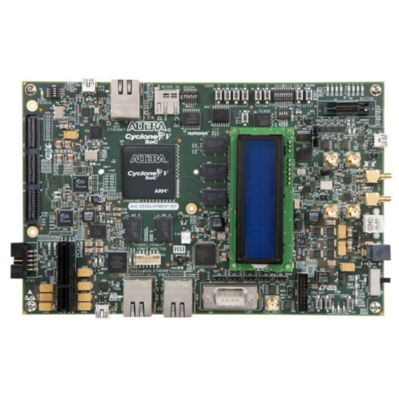
Cyclone V SoC Development Kit and SoC Embedded Design Suite
- Brand: Terasic
- Product Code: Cyclone V SoC Development Kit and SoC Embedded Design Suite
- Availability: In Stock
The Altera® Cyclone® V SoC Development Kit offers a quick and simple approach to develop custom ARM® processor-based SOC designs accompanied by Altera’s low-power, low-cost Cyclone V FPGA fabric. This kit supports a wide range of functions, such as:
Processor and FPGA prototyping and power measurement
Industrial networking protocols
Motor control applications*
Acceleration of image- and video-processing applications*
PCI Express® (PCIe®) x4 lane with ~1,000 MBps transfer rate (endpoint or rootport)
*Application-specific daughtercards, available separately, supporting a wide range of I/O and interface standards.
Linux community portal : RocketBoards.org
Specifications
Featured devices
Cyclone V SX SoC—5CSXFC6D6F31C6N (SoC)
MAX®V CPLD—5M2210ZF256C4N (system controller)
MAX II CPLD—EPM570GF100 (embedded USB-BlasterTMII cable)
FPGA configuration sources
Embedded USB-Blaster II (JTAG) cable
EPCQ flash (PFL)
Hard processor system (HPS)
FPGA memory
1 GB DDR3 SDRAM (32 bit)
FPGA I/O interfaces
2X 10/100 Ethernet PHYs (EtherCAT)
PCIe Gen 1 x4 female connector
Universal high-speed mezzanine card (HSMC)—x4 transceivers, x16 TX LVDS, x16 RX LVDS
One serial digital interface (SDI) channel
Four SMAs for one transceiver channel
x4 push buttons
x2 switches
x4 LEDs
HPS boot sources
128 MB QSPI Flash
Removable Micro-SD Card flash
FPGA
HPS memory
1 GB DDR3 SDRAM (32 bit) with error correction code (ECC)
128 MB QSPI flash
Micro-SD Card socket with 4 GB Micro-SD Card flash device
HPS I/O interfaces
x1 USB 2.0 On-the-Go (OTG)
x1 10/100/1000 Gigabit Ethernet (10GbE/100GbE/1000GbE)
x1 CAN
x1 UART (UART to USB bridge)
x1 real-time clock (with battery backup)
x1 two-line text LCD
1-/2-channel, 20 bit delta-sigma analog-to-digital converter (Linear Technology LTC2422)
x4 push buttons
x4 switches
x4 LEDs
Clocking
Four-output programmable clock generator for FPGA reference clock inputs
125 MHz LVDS oscillator for FPGA reference clock input
148.5 MHz LVDS programmable voltage-controlled crystal oscillator (VCXO) for FPGA reference clock input
50 MHz single-ended oscillator for FPGA and MAX V FPGA clock input
100 MHz single-ended oscillator for MAX V FPGA configuration clock input
SMA input for HPS clock
Power
Laptop DC input 14—20 V adapter
System monitoring circuit
Power (voltage, current, wattage)
HSMC breakout board
HSMC loopback board
Mechanical
Board dimensions—8.19” x 5.22”
Cyclone V SX FPGA Development Kit software content
Design examples
Board test system (BTS)*
Golden System Reference Design with Board Update Portal web server
Complete documentation
SoC Embedded Design Suite Subscription Edition
ARM Development Studio 5 (DS-5™) Altera Edition Toolkit
Hardware-to-software handoff tools
Linux run-time software for application development
SoC hardware libraries for firmware development
Application examples
Free software supported by Quartus®II software v13.1, Web Edition
* Watch the video to learn more.
Schematic of the Cyclone V SX SoC Development Board

Related Products

VEEK-MT2-C5SoC
Rp.50,685,000.00

VEEK-MT2-C5SoC Upgrade Kit
Rp.9,630,000.00
Tags: SoC Platform, Development Board, Intel, FPGA, Cyclone V SoC Development Kit and SoC Embedded Design Suite, Terasic