


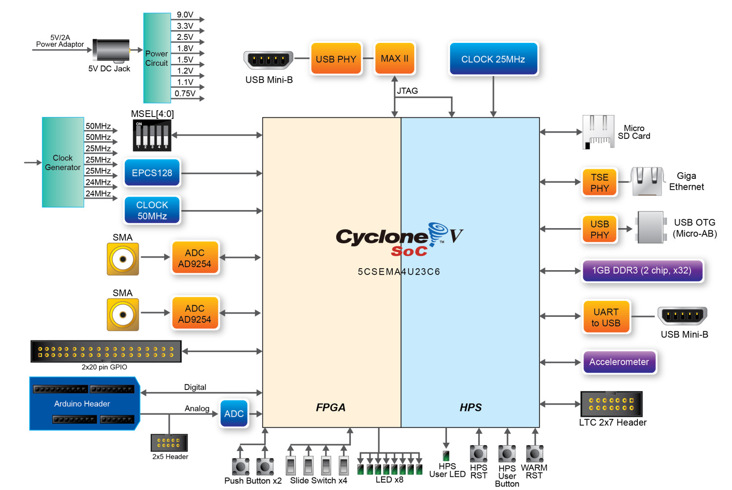
The ADC-SoC is a SoC FPGA motherboard with dual-channel high-speed ADC. The main card is based on the Terasic DE0-Nano-SoC board with a built-in high-speed ADC circuit on the DCC (AD / DA Data Conversion Card) on top of the main card. This feature makes the board an ideal platform for systems that require high-speed ADC applications.
The built-in ADC circuit uses SMA as the input interface. The circuit provides two channels, each with 14-bit resolution and a sample rate of up to 150 MSPS (Megasamples per Second).
Component Solutions for Altera FPGAs

|
|
| ▲ Power Solution | ▲ SDRAM Memory Solution |

|
|
| ▲ Ethernet Solution | ▲ Inductive Component Solution |

|

|
| ▲ Capacitive Component Solution | ▲ Accelerometer Solution |
Specification
The ADC-SoC board has many features that allow users to implement a wide range of designed circuits, from simple circuits to various multimedia projects.
The following hardware is provided on the board:
FPGA Device
- Altera Cyclone® V SE 5CSEMA4U23C6N device
- Serial configuration device – EPCS128
- USB-Blaster II onboard for programming; JTAG Mode
- 2 push-buttons
- 4 slide switches
- 8 green user LEDs
- Three 50MHz clock sources from the clock generator
- One 40-pin expansion header
- One Arduino expansion header (Uno R3 compatibility), can connect with Arduino shields
- One 10-pin Analog input expansion header (shared with Arduino Analog input)
- A/D converter, 4-pin SPI interface with FPGA
- Two 14-bit AD Converters with 150 MSPS (Mega-Samples per Second)
HPS (Hard Processor System)
- 925MHz Dual-core ARM Cortex-A9 processor
- 1GB DDR3 SDRAM (32-bit data bus)
- 1 Gigabit Ethernet PHY with RJ45 connector
- USB OTG Port, USB Micro-AB connector
- Micro SD card socket
- Accelerometer (I2C interface + interrupt)
- UART to USB, USB Mini-B connector
- Warm reset button and cold reset button
- One user button and one user LED
- LTC 2x7 expansion header
- On-Board RTC (Real-Time Clock)
HIgh Speed AD (Analog-to-Digital) Conversion
- Two channels
- 14-bit resolution
- Up to 150MSPS (Mega-Samples per Second)
Block Diagram of the ADC-SOC Board
Kit Contents
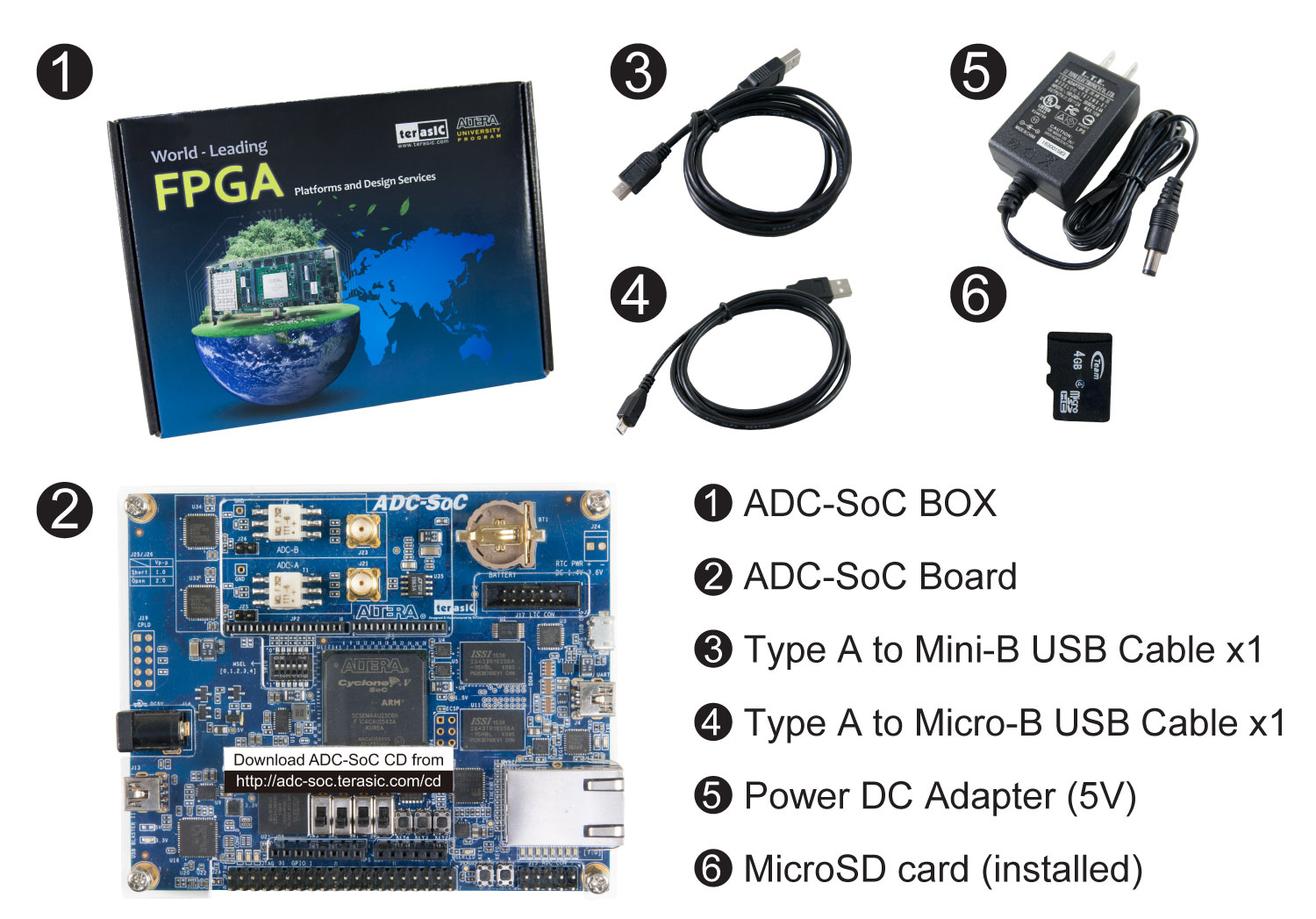
The accessories might not look exactly the same as shown on this webpage
Tags: SoC Platform, Intel, FPGA, ADC-SoC, Terasic